
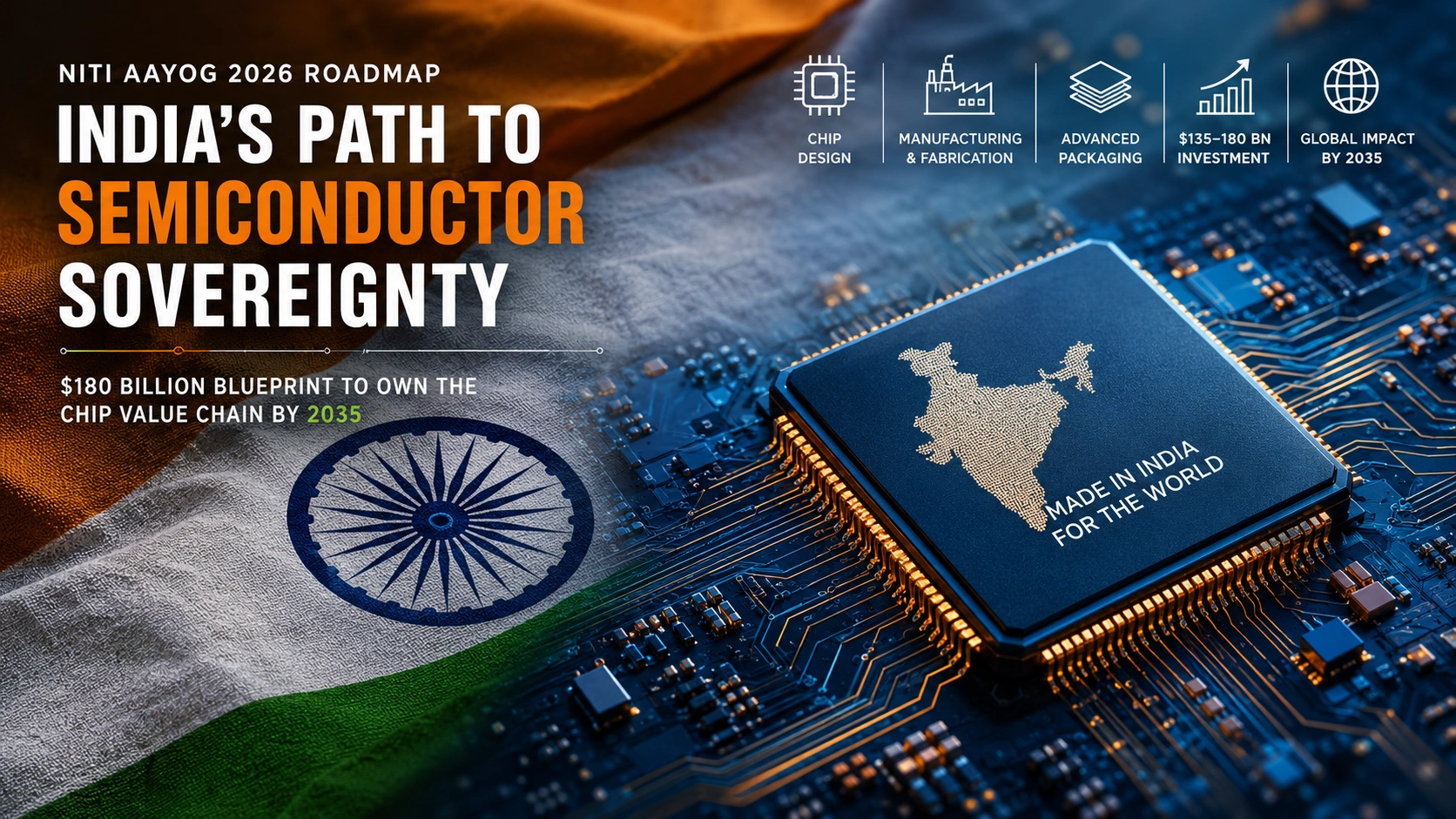
India’s Semiconductor Sovereignty: Decoding NITI Aayog’s $180 Billion Blueprint to Strengthen the Chip Value Chain
A country that depends heavily on imported chips cannot build a $5 trillion economy without strengthening its own semiconductor ecosystem. NITI Aayog’s new roadmap makes that argument clearly, and with unusual urgency.
Data at a glance
- 90–95% of India’s current semiconductor demand is met through imports.
- $150 billion was spent on semiconductor imports between FY2017 and FY2025.
- $90 billion is projected domestic semiconductor demand by FY2030.
- More than $200 billion is projected domestic demand by FY2035.
- $135–180 billion is the cumulative investment required over the next decade.
- $120–150 billion is the target semiconductor value chain India must build by 2035.
- $1.5 trillion+ is the expected size of the global semiconductor market by 2035.
- 33% is the minimum share of required investment the Government of India should anchor.
The import dependence challenge
Every time an Indian smartphone powers on, a 5G tower begins operating, or an electric vehicle moves into production, a semiconductor is doing essential work in the background. In most cases, that chip was designed abroad, manufactured overseas, and packaged elsewhere before reaching India.
NITI Aayog’s Frontier Tech Hub, which released its report Future of India’s Semiconductor Industry on 30 May 2026, puts a firm number on this dependence. Between FY2017 and FY2025, India spent nearly $150 billion importing semiconductor products. That is a large and growing outflow, and it highlights how dependent the country remains on external supply chains.
The report also notes that India’s semiconductor demand is growing at around 19% annually, one of the fastest rates globally. By FY2030, domestic demand could reach about $90 billion, and by FY2035 it may cross $200 billion. If the country continues on its present path, annual import costs could become significantly larger over time.
Finance Minister Nirmala Sitharaman, who released the report, said India must move from being a major consumer of chips to becoming a more important part of the global semiconductor value chain. NITI Aayog Vice Chairman Ashok Kumar Lahiri also warned that excessive dependence on imported black-box technologies could limit India’s long-term strategic autonomy. The core message is straightforward: semiconductor capability is becoming a matter of economic strength and strategic resilience.https://thequantiq.com/indian-rupee-depreciation-ai-economy/
The global shift
The timing of the report matters because the semiconductor industry itself is changing. Global semiconductor revenues reached $631 billion in 2024, and the market is projected to grow steadily over the next decade. By 2030, global sales may cross $1 trillion, and by 2035, the figure could reach $1.5 trillion.
At the same time, the industry is moving from a simple focus on transistor shrinkage to more complex, application-specific chip architectures. AI accelerators, NPUs, GPUs, and domain-specific processors increasingly depend on advanced packaging, chiplets, and 2.5D or 3D integration.
This shift is important for India because it opens a more accessible path into the industry. The race is no longer only about building the most advanced fabrication plants. It is also about who can assemble, integrate, and package chips efficiently and reliably.
That is where India may have a realistic opportunity to build strength without trying to match the most advanced foundries node for node.
Why not the foundry race
The report’s central strategic point is that India should not try to replicate the full advanced foundry model already dominated by leaders such as TSMC and Samsung. Competing directly at the bleeding edge of transistor miniaturisation would require enormous capital, very long time horizons, and no guarantee of success.
Instead, the roadmap recommends building strength in parts of the value chain where India has clearer advantages and where demand is likely to grow quickly.
Advanced packaging and OSAT
Outsourced semiconductor assembly and test, or OSAT, refers to the process of assembling fabricated wafers into finished chips. Advanced packaging includes chiplets, 2.5D integration, and 3D stacking, and it is becoming one of the most important areas in chip performance.
NITI Aayog recommends that India aim to become a top-three global destination for advanced packaging and OSAT by 2035. India already has a strong engineering base, cost advantages, and a growing domestic demand pool. Early projects such as the Tata Electronics-Powerchip Semiconductor partnership in Dholera and CG Power’s OSAT facility in Sanand point in that direction.
Compound semiconductors: SiC and GaN
Silicon carbide (SiC) and gallium nitride (GaN) are wide-bandgap semiconductors that can handle higher temperatures, higher voltages, and faster switching speeds than standard silicon chips. These properties make them especially important for electric vehicles, 5G systems, solar inverters, railway traction, and defence electronics.
India’s domestic demand for these chips is likely to rise as EV manufacturing, renewable energy, 5G rollout, and defence modernisation expand. The report suggests that India should develop dedicated compound semiconductor fabrication capacity rather than relying entirely on imports.
Specialty analog and mixed-signal chips
Not every semiconductor needs to be a cutting-edge logic chip. Industrial automation, medical devices, automotive sensors, smart metering, and agricultural IoT all depend on mature-node analog and mixed-signal chips.
These chips may receive less attention than advanced processors, but they remain essential to manufacturing and infrastructure. India’s expanding industrial base creates a practical demand environment for domestic production in this segment.
Semiconductor design IP
India already hosts a large share of the world’s semiconductor design workforce. Global companies such as Qualcomm, Intel, Texas Instruments, and ARM operate major R&andD centres in Bengaluru, Hyderabad, and Pune. However, much of this talent works on designs owned by foreign firms.
The report calls for more investment in sovereign semiconductor design intellectual property — in other words, chip architectures that India can own, license, and build on. That would move the country closer to the highest-value part of the semiconductor chain.
Five pillars of strategy
| Pillar | What India needs to do |
| Frontier R&D | Build domestic semiconductor design IP, invest in advanced node research, and compete in proprietary chip architectures for AI and 5G/6G workloads. |
| Policy & Investment | Create a 10-year predictable policy horizon and a broader incentive framework supported by a national nodal agency. |
| Production | Focus on advanced packaging, chiplet integration, compound semiconductor fabs, and secure manufacturing for strategic sectors. |
| People | Build a full talent pipeline covering technicians, engineers, packaging specialists, materials scientists, and architects. |
| Partnerships | Strengthen trusted supply chain alliances with the US, Japan, the EU, and resource-rich countries. |
The value of this framework lies in its interdependence. Investment without talent can leave facilities underused. Talent without policy stability can result in migration. Production without partnerships can create supply bottlenecks.
The report’s strongest point is that India needs to develop these pillars together, not one after another.
Financing the shift
Semiconductor fabrication is among the most capital-intensive industries in the world. A single advanced fab may cost $10 billion to $20 billion, take years to build, and require constant upgrades to remain competitive.
For that reason, the report recommends total investments of $135 billion to $180 billion across the semiconductor value chain over the next decade. That includes design, fabrication, advanced packaging, materials, and enabling infrastructure.
The report also recommends that the Government of India anchor at least one-third of the total requirement, or roughly $45 billion to $60 billion, to reduce risk and attract private capital.
That approach is consistent with global precedent. The US CHIPS and Science Act, the European Chips Act, and Japan’s support for TSMC all show that semiconductor ecosystems typically need strong public backing before private capital follows at scale.
The report further argues for an autonomous national semiconductor nodal agency. Such a body could provide continuity, technical oversight, and policy stability across political cycles. That institutional recommendation may be as important as the financial one.
Materials and supply risks
Semiconductors depend on much more than silicon. Their manufacture requires specialty chemicals, rare earth elements, advanced gases, and other materials that are often concentrated in a small number of countries.
Gallium and germanium, both important for compound semiconductors, are heavily processed in China. Cobalt, used in some memory chip manufacturing, is concentrated in the Democratic Republic of Congo. Silicon carbide substrates also depend on scarce high-purity inputs.
The report therefore emphasises the need for trusted partnerships with countries such as the Netherlands, Japan, and the United States, particularly for equipment, advanced materials, and design tools. In that sense, India’s credibility as a semiconductor partner will depend not just on policy announcements, but on its ability to build real manufacturing capacity.
The Quantiq assessment
The NITI Aayog report is a serious and useful strategic document. Its main strength is that it recognises India should not try to win every part of the semiconductor race in the same way. Instead, it points toward areas such as advanced packaging, compound semiconductors, and design IP, where India may have a better chance of building durable strength.
The investment logic is also grounded in international precedent. The scale may be large, but it is broadly in line with how other major economies have supported semiconductor development.
The most important unresolved question is institutional continuity. Without a durable national agency and stable policy framework, even a well-designed roadmap can lose momentum.
For Northeast India, the report is only a starting point. The region’s role in the semiconductor value chain will depend on how states, universities, and industry actors align with the broader national push. Engineering talent, energy infrastructure, and industrial planning could all become relevant if the region positions itself early.
The Quantiq will continue tracking how semiconductor policy unfolds, with a particular focus on how the Northeast can connect to talent development, packaging, materials, and energy-linked manufacturing.https://thequantiq.com/india-315-billion-tech-sector-northeast-ai-economy/
Frequently asked questions
What is the NITI Aayog semiconductor report?
Future of India’s Semiconductor Industry was released by NITI Aayog’s Frontier Tech Hub on 30 May 2026. It is a 10-year roadmap for building India’s semiconductor ecosystem across design, fabrication, packaging, talent, materials, and international partnerships.
Why does India import most of its semiconductors?
India’s semiconductor manufacturing base is still at an early stage. For many years, the country focused more on design services than on manufacturing, while global fabrication remained concentrated in Taiwan, South Korea, the United States, and parts of East Asia.
Why does advanced packaging matter?
Advanced packaging is increasingly where performance gains are achieved in AI chips and other complex processors. It also requires less capital than leading-edge fabrication, which makes it a more practical entry point for India.
What are SiC and GaN semiconductors?
SiC and GaN are wide-bandgap compound semiconductors that can tolerate high voltage, heat, and switching speeds. They are important for EVs, 5G systems, renewable energy, and defence electronics.
How does this affect Northeast India?
Northeast India is no longer just a passive consumer; it is now a direct participant in the global value chain through the Tata Semiconductor assembly and test facility being set up at Jagiroad in Assam. This ₹27,000-crore project places the region firmly on the microelectronics map. Future opportunities will expand through energy-linked industrial zones, specialized engineering curriculum in regional institutions, and a localized supply ecosystem for materials and logistics. The region’s long-term success will depend on proactive state planning to support this anchor asset.
Strategic Intelligence & Primary Sources
Official Policy Document: Future of India’s Semiconductor Industry (Published May 2026
Issuing Authority: NITI Aayog, Frontier Tech Hub, Government of India
Direct Data Access: https://niti.gov.in/sites/default/files/2026-05/Future-of-India-Semiconductor-Industry.pdf






One Comment