India’s Semiconductor Moment
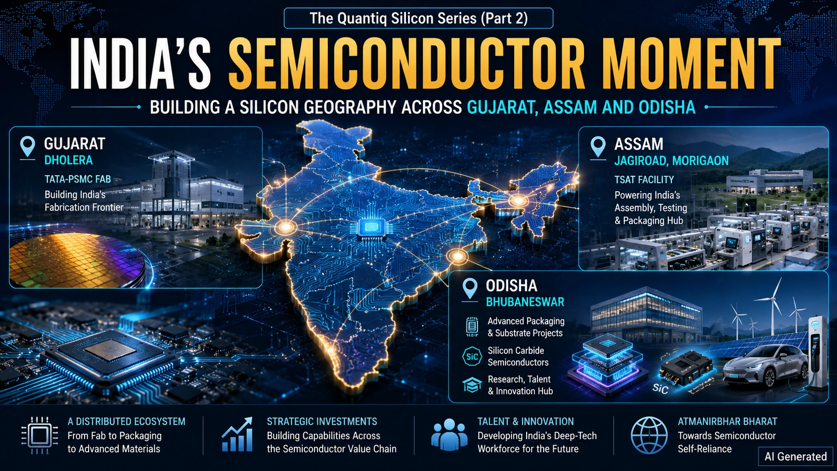
From Dholera to Morigaon and Bhubaneswar: Building India’s Silicon Geography
For decades, India participated in the global semiconductor industry primarily as a source of engineering talent.
Indian engineers designed chips for global companies. They built software tools, managed research centres and powered innovation pipelines. Yet the physical infrastructure of the semiconductor economy largely existed elsewhere.
That is beginning to change.
Through the India Semiconductor Mission (ISM) 2.0, a combination of policy incentives, strategic investments and geopolitical realignments is helping India build capabilities across the semiconductor value chain. The country’s ambitions now extend beyond design into fabrication, assembly, testing, advanced packaging and specialised semiconductor materials.
Three regions illustrate this transformation particularly well.
Gujarat is becoming India’s fabrication frontier.
Assam is entering the semiconductor assembly and testing ecosystem.
Odisha is emerging as a hub for advanced packaging, substrates and compound semiconductors.
Together, they offer a glimpse of India’s evolving semiconductor geography—and its attempt to secure a place in one of the world’s most strategic industries.
Why India Entered the Semiconductor Race
The semiconductor shortages that followed the COVID-19 pandemic delivered a harsh lesson to governments around the world.
Modern economies depend on semiconductors.
Without chips, automobile production slows. Consumer electronics become scarce. Telecommunications infrastructure faces disruptions. Defence systems become vulnerable.
The crisis exposed how heavily the world relied on a concentrated group of manufacturers and suppliers.
For India, the lesson was particularly important.
The country represented one of the world’s largest technology markets and one of its largest engineering talent pools, yet it remained heavily dependent on imported semiconductors.
That dependence carried economic, technological and strategic risks.
As geopolitical tensions intensified and global supply chains diversified, India saw an opportunity to move beyond being a participant in semiconductor design and become a stakeholder in semiconductor manufacturing.
The result was the India Semiconductor Mission.https://thequantiq.com/silicon-sovereignty-wars-ai-chip-industry/
ISM 2.0 — The National Blueprint
The India Semiconductor Mission 2.0 represents one of the most ambitious industrial initiatives undertaken by the country in recent decades.
Unlike earlier efforts that focused primarily on electronics assembly, ISM 2.0 seeks to build a complete ecosystem.
The objective is not merely to manufacture chips.
It is to create an integrated semiconductor value chain encompassing design, fabrication, packaging, testing, materials, equipment and talent development.
More than a dozen semiconductor-related projects have already been approved across multiple states, backed by investments running into billions of dollars.
While India still remains years away from competing with the world’s leading semiconductor powers, the direction of travel is becoming increasingly clear.
The country intends to become a serious player.
Gujarat: Building India’s First Silicon Frontier
No state better symbolises India’s semiconductor ambitions than Gujarat.
Tata-PSMC Dholera Fab
The Tata Electronics semiconductor fabrication facility at Dholera, developed in partnership with Taiwan’s Powerchip Semiconductor Manufacturing Corporation (PSMC), represents India’s most ambitious semiconductor manufacturing project to date.
The facility will initially focus on mature process nodes rather than cutting-edge 2nm or 3nm technologies.
Some observers view this as a limitation.
In reality, it is a pragmatic strategy.
Most global semiconductor demand still comes from mature-node applications including automotive electronics, industrial automation, telecommunications equipment and consumer devices.
Building manufacturing expertise at these nodes provides India with an opportunity to develop operational experience, supply-chain capabilities and talent pipelines before pursuing more advanced technologies.
The significance of Dholera therefore extends beyond the chips it will produce.
It represents India’s entry into the fabrication business itself.
For a country that has spent decades discussing semiconductor manufacturing, Dholera is where ambition begins to become reality.
Assam: Northeast India’s Semiconductor Moment
For readers of The Quantiq, one project carries particular significance.
TSAT Jagiroad and the Rise of Morigaon
The Tata Semiconductor Assembly and Test (TSAT) facility at Jagiroad in Morigaon district marks Northeast India’s entry into the global semiconductor ecosystem.
Unlike a fabrication facility, TSAT will focus on semiconductor assembly, packaging and testing—critical stages that transform manufactured wafers into finished chips ready for deployment across industries.
The project is historic for Assam.
For decades, industrial development in Northeast India has largely revolved around traditional sectors such as tea, oil, natural gas and agriculture.
Semiconductors represent an entirely different category of opportunity.
The arrival of TSAT places Assam within a global industry that sits at the centre of artificial intelligence, advanced electronics, telecommunications and defence technologies.
Its significance is not merely economic.
It is psychological.
For young people across the Northeast, semiconductor manufacturing is no longer an abstract concept associated with Silicon Valley, Taiwan or South Korea.
It is becoming part of their own industrial landscape.
Whether TSAT evolves into a larger semiconductor cluster remains to be seen.
But it has already accomplished something important: it has placed Northeast India on the semiconductor map.
Odisha: India’s Emerging Packaging and Compound Semiconductor Hub
While Gujarat and Assam have attracted considerable attention, another state is quietly assembling a semiconductor ecosystem of its own.
That state is Odisha.
The Intel–3DGS Opportunity
Recent announcements involving advanced semiconductor substrate manufacturing have elevated Odisha’s profile within India’s semiconductor ambitions.
Substrates form a critical component of advanced chip packaging, providing the foundation that connects semiconductor dies to electronic systems.
As AI workloads become more demanding, advanced packaging technologies are becoming increasingly important.
This trend is creating opportunities beyond traditional fabrication.
Odisha appears determined to seize them.
Advanced Packaging and the Next Semiconductor Frontier
Industry experts increasingly argue that future performance gains will depend as much on advanced packaging as on transistor miniaturisation.
Technologies involving 3D stacking, chiplets and high-bandwidth interconnects are becoming central to AI infrastructure.
Projects being developed in Odisha position the state within precisely this segment of the value chain.
Rather than competing directly with fabrication hubs, Odisha is targeting areas where future demand is expected to expand rapidly.
Silicon Carbide and the EV Revolution
Odisha is also emerging as a potential centre for Silicon Carbide (SiC) semiconductors.
Unlike traditional silicon chips, Silicon Carbide devices are particularly valuable for electric vehicles, renewable energy systems, industrial power electronics and advanced defence applications.
As global demand for electrification accelerates, Silicon Carbide is expected to become one of the fastest-growing segments of the semiconductor industry.
By attracting investment into this area, Odisha is positioning itself at the intersection of semiconductors, clean energy and advanced manufacturing.
Why Bhubaneswar Matters
Beyond manufacturing projects, Odisha is also investing in research, talent development and semiconductor education.
This matters because semiconductor ecosystems cannot be built solely through factories.
They require engineers, researchers, universities, suppliers and innovation networks.
Bhubaneswar’s growing role as a technology and innovation hub could therefore prove just as important as any individual investment announcement.
The state’s long-term ambition appears clear: build not merely projects, but an ecosystem.
India’s Strengths
India enters the semiconductor race with several structural advantages.
The country possesses one of the largest semiconductor design talent pools in the world.
Global technology companies already operate major design centres in Bengaluru, Hyderabad, Chennai and other cities.
India also offers a rapidly expanding domestic market for electronics, electric vehicles and digital infrastructure.
At the same time, geopolitical diversification is creating demand for trusted semiconductor partners outside existing manufacturing hubs.
These factors provide India with a meaningful foundation on which to build.
India’s Gaps
Yet significant challenges remain.
India lacks deep experience in advanced semiconductor fabrication.
Critical supply chains involving semiconductor-grade chemicals, specialty gases and manufacturing equipment are still developing.
Access to leading-edge lithography technologies remains limited.
Most importantly, building a globally competitive semiconductor ecosystem requires patience.
Countries such as Taiwan, South Korea and Japan spent decades building capabilities that cannot be replicated overnight.
India’s semiconductor journey will therefore be measured in decades rather than years.
The Quantiq’s Assessment
A common mistake is to view India’s semiconductor ambitions through the lens of a single project.
That is not what is happening.
India is not building one semiconductor city.
It is building a semiconductor geography.
Gujarat is emerging as the fabrication frontier.
Assam is entering assembly and testing.
Odisha is building capabilities in advanced packaging, substrates and compound semiconductors.
Meanwhile, states such as Karnataka, Telangana and Tamil Nadu continue strengthening India’s design and electronics ecosystems.
Viewed individually, these projects may appear modest compared to Taiwan, South Korea or the United States.
Viewed collectively, they tell a different story.
They suggest that India is slowly assembling the pieces of a semiconductor ecosystem that did not exist a decade ago.
The journey remains long.
The challenges remain significant.
But for the first time, the map is beginning to take shape.
In Part 3 of The Quantiq Silicon Series, we examine Netrasemi’s breakthrough AI chip, the rise of India’s fabless semiconductor ecosystem, and the growing debate over whether the AI boom is creating the largest technology bubble since the dot-com era.https://thequantiq.com/northeast-india-green-industrialisation-bamboo-manufacturing/


2 Comments